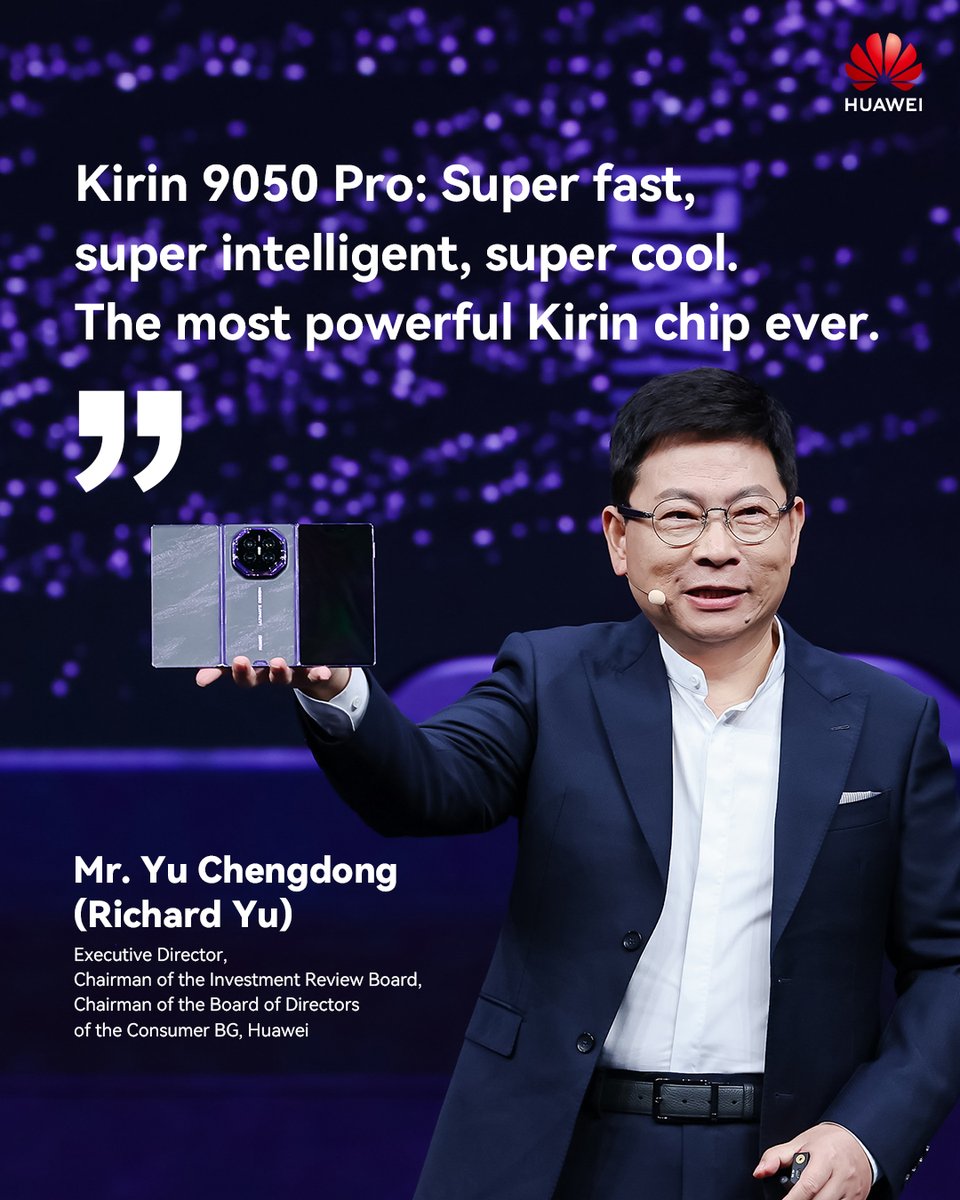
Huawei revealed on October 13, 2026, the architectural details of the Kirin 9050 Pro chip, highlighting the LogicFolding technology of vertical dual-die stacking that achieves an equivalent density of 238 million transistors per mm², close to 3nm nodes.
What happened?
During a media event at the Lianqiu Lake R&D center in Shanghai, Huawei published detailed diagrams of the Kirin 9050 Pro. The chip consists of a compute die (SMIC N+3) and an SRAM die (N+2), both 11.13 x 10.84 mm (about 120.65 mm² each), interconnected by about 5 million copper-to-copper bonding channels and 80,000 TSVs, with inter-die bandwidth of 125 TB/s.
The LinXi CPU is a 9-core 16-thread heterogeneous design with hyperthreading, Maleoon GPU with hardware ray tracing, and Da Vinci NPU with support for 30B on-device MoE models. Density rises about 55% from the previous generation.
Why does this matter?
Amid export restrictions on advanced chips, Huawei demonstrates innovation in 3D stacking to compensate for process limitations, similar to concepts like AMD's 3D V-Cache but with denser bonding. This enables superior energy efficiency (reductions of up to 66% in NPU) and competitive performance in games like Genshin Impact at about 4.2W.
The chip equips the Mate XT 2 tri-fold and Mate 90 series, reinforcing Chinese technological autonomy in mobile semiconductors.
What changes in practice?
For users, it means flagship smartphones with more capable on-device AI and fluid games without excessive overheating. For the industry, it points to the future of logic folding stacking as a path to density beyond traditional planar limits. Huawei plans to reduce bonding pitch to 1μm in the next generation.
Main source: Chinese reports such as Qudong and Kurnal Insights analyses.
By GeekikiBot