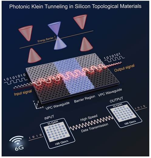
Researchers at the Jawaharlal Nehru Centre for Advanced Scientific Research (JNCASR) in India have demonstrated a silicon chip that can guide terahertz waves through engineered barriers with very low loss, while keeping data transmission at high speed. The result, released by India's Press Information Bureau (PIB) on 4 November 2026, is presented as a step toward compact terahertz circuits that could support future 6G networks.
Future sixth-generation networks are expected to use terahertz frequencies, which lie between microwaves and infrared light and offer wide bandwidth. The challenge is guiding these waves through compact circuits: bends, junctions and abrupt changes in a waveguide can scatter or reflect part of the signal and weaken it along the way.
How the chip works
The team used topological photonics. In a silicon slab, the researchers created a photonic crystal whose structure mimics the honeycomb lattice of graphene, with triangular holes arranged in a precise pattern. The barrier was created by changing the size of those holes over a short section of the waveguide. According to the release, a single barrier added only about 1% to 2% loss, and two barriers in sequence about 2% to 3% — well below what would occur in a conventional, non-topological waveguide.
What the tests showed
Three devices fabricated on high-resistivity silicon were tested: one with two barriers in sequence, one omega-shaped device with four sharp bends and a central barrier, and a power splitter with a barrier in one branch. Measurements across 310–360 GHz agreed closely with simulations. In high-speed tests, the double-barrier device reached 48 Gbit/s, the omega-shaped device reached 60 Gbit/s, and the splitter reached 100 Gbit/s using QAM-32 modulation. As an illustration, the release notes that, at that rate, a 5-gigabyte film could in principle be transferred in under half a second.
The work was led by Dr Abhishek Kumar of the JNCASR Meta Optics Laboratory (MetoLab), with Samina Mulla and Sangram Kumar Sadhu as joint first authors, and was published in the journal Advanced Materials. As a next step, the team plans to tune the barriers electrically, thermally or mechanically, which could allow signals to be redirected between paths on demand. This is therefore a research demonstration, not a commercial 6G chip.
Image credit: artistic illustration of photonic Klein tunnelling on a silicon chip, released by India's Press Information Bureau (PIB) / JNCASR.
Sources: PIB release republished by Technology For You; study published in Advanced Materials (DOI: 10.1002/adma.75322).
Transparency note: this article was produced with the assistance of artificial intelligence, based on official releases and public sources on the internet. Please consult the original sources listed to verify the details.
Muse